


+86 13603063656
Printed circuit boards (PCBs) are the backbone of nearly every electronic device, but what exactly is a PCB made of? Understanding PCB materials isn’t just useful for engineers—it’s critical for OEMs, sourcing managers, and product designers in any B2B setting. But here’s the kicker… material selection directly impacts electrical performance, cost, thermal stability, and even compliance with safety regulations. In this Jerico Multilayer PCB supplier writed guide, we’ll peel back every layer of a PCB, from substrates and copper to solder masks and specialty compounds. If you’ve ever wondered what your boards are really made of, this is your complete breakdown.
What Is PCB Made Of
Let’s get started by unpacking the PCB’s material anatomy.
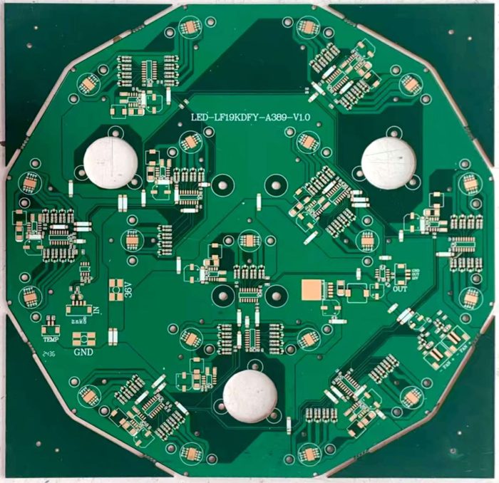
A PCB is more than just a flat green board. It’s a carefully engineered sandwich of materials—each chosen for its specific function. You’ve got substrates to hold everything together, copper for electrical connectivity, solder masks for protection, and silkscreens for guidance. Each layer serves a purpose, and using the wrong material can lead to heat failure, signal distortion, or regulatory noncompliance.
But what’s the real story? Most people don’t realize how tailored each board’s composition can be. A high-frequency telecom board will look nothing like a consumer gadget board. Likewise, military PCBs often include exotic, heat-resistant compounds.
Whether you’re designing for automotive, medical, or IoT, the right mix of materials determines everything from signal clarity to longevity. That’s why it pays to get familiar with what a PCB is made of—because when you understand your layers, you build a better product.
| PCB Layer | Material Function | Typical Materials Used |
| Substrate | Structural base | FR4, polyimide, ceramic |
| Conductive Layer | Electrical signal routing | Copper foil |
| Dielectric | Insulation between layers | Epoxy resin, ceramic blend |
| Solder Mask | Protection & insulation | Epoxy, LPI green mask |
| Silkscreen | Component labeling | Epoxy-based white ink |
| Finish Layer | Surface protection & soldering | ENIG, HASL, OSP |
Ready for the good part? The heart of any PCB is its multi-layered structure.
A standard PCB typically consists of a non-conductive substrate, one or more layers of copper foil, a solder mask, silkscreen markings, and a surface finish. The number of copper layers may vary depending on the application—from simple single-sided PCBs to complex 12+ layer multilayer boards.
The inner core, usually made from FR4, gives the board rigidity and strength. On either side of this core, copper layers are laminated under high pressure and temperature. Dielectric layers separate each copper sheet to prevent short circuits. Over these, the solder mask protects traces from corrosion and shorts. Finally, a silkscreen helps identify components during assembly.
But here’s the kicker… even small changes in this stack-up can affect signal integrity, impedance, and thermal performance. That’s why material selection isn’t just cosmetic—it’s critical engineering.
For example, a medical-grade ECG monitor might use a 6-layer board with a polyimide core for flexibility and biocompatibility. In contrast, a consumer router may use a 2-layer FR4 stack with ENIG finish for cost-effectiveness.
| Layer | Purpose | Material Example |
|---|---|---|
| Core Substrate | Mechanical stability | FR4, polyimide, ceramic |
| Copper Layer | Signal/power transmission | Electro-deposited copper |
| Prepreg (dielectric) | Electrical insulation | Epoxy resin |
| Solder Mask | Oxidation & short prevention | LPI green mask |
| Silkscreen | Labeling/assembly aid | White epoxy ink |
| Surface Finish | Solderability & protection | HASL, ENIG, OSP |
Now, let’s dive into the real foundation of your PCB.
The substrate forms the physical base of the board, and its characteristics determine how well your PCB handles heat, vibration, moisture, and frequency. The most common material? FR4, a flame-retardant woven glass epoxy laminate. But depending on the application, other materials may be better suited.
Here’s the key point: Substrate selection is not about choosing the most expensive or the cheapest option—it’s about finding the best fit for your product’s requirements.
Let’s break it down:
| Substrate Type | Key Properties | Ideal Applications | Cost Level |
|---|---|---|---|
| FR4 | Flame-retardant, cost-effective, good electrical insulation | Consumer electronics, industrial controls | Low |
| CEM-1/CEM-3 | Low cost, moderate strength, cellulose-epoxy blend | Lighting, toys, low-end electronics | Very Low |
| Polyimide | High-temperature resistance, flexible, excellent durability | Aerospace, automotive, flexible circuits | High |
| Ceramic | Extreme heat resistance, superior RF performance | Military, high-power modules, RF/microwave | Very High |
Key Takeaways:
Remember: The best material isn’t necessarily the most expensive—it’s the one that aligns with your product’s electrical, thermal, and mechanical demands while balancing cost efficiency.
4. Copper Foil Layers and Their Function
Let’s move up the stack—literally.
The copper foil is what makes the PCB conduct. These layers form the electrical paths (traces) between components. Without them, your PCB is just a pretty plastic sheet. But here’s the kicker… copper thickness, purity, and patterning all affect performance.
Typically, copper is laminated onto the substrate via heat and adhesive. The standard thickness is 1 oz (35μm), but you’ll see 0.5 oz to 6 oz used depending on the current load.
Thicker copper = higher current handling. That’s why power electronics, EV charging modules, and industrial motor controllers use heavy copper boards.
Three examples:
| Copper Thickness | Typical Use Case | Notes |
|---|---|---|
| 0.5 oz | Signal transmission, low power | Great for cost savings |
| 1 oz | Standard in most PCBs | Balanced performance |
| 2 oz | LED, motor drivers, battery PCBs | Better heat management |
| 3+ oz | Industrial power & automotive | Specialized, more expensive |
Let’s talk insulation—it’s not just about heat; it’s about safety and signal integrity.
Dielectric layers separate copper traces to prevent short circuits and allow multilayer PCBs to function without interference. But here’s where it gets interesting… the material and thickness of these layers affect capacitance, impedance, and even EMI performance.
Common dielectric materials include:
● Epoxy Resin: Most widely used with FR4. It’s cost-effective and thermally stable up to 130°C.
● Ceramic-filled PTFE: Used in RF and microwave applications. Offers high signal integrity and low loss.
● Rogers Materials: Known for consistent dielectric constants and low dissipation. Ideal for aerospace and telecom.
Three real-world examples:
| Dielectric Type | Dielectric Constant (Dk) | Application |
|---|---|---|
| FR4 (Epoxy) | ~4.2–4.5 | Standard electronics |
| Ceramic-filled PTFE | ~2.2–2.5 | High-frequency RF/microwave |
| Rogers RO4350B | 3.48 | Aerospace, telecom |
| Polyimide | ~3.4 | Flex PCBs and extreme temps |
Now, let’s address that iconic green layer—what is it and why does it matter?
The solder mask is more than a pretty coat. It insulates copper traces, prevents oxidation, and reduces the risk of solder bridging during assembly. But here’s the kicker… while green is the industry default, it’s far from the only option.
Manufacturers now offer solder masks in red, black, white, blue, and even transparent for aesthetic or identification purposes. What doesn’t change is the need for precision. Solder mask misalignment can cause short circuits or exposed copper that corrodes.
Most solder masks are LPI (Liquid Photo-Imageable) epoxy, cured under UV light. Some advanced boards use dry film masks for better edge definition in high-density layouts.
Three use cases:
| Solder Mask Color | Common Use Cases | Notes |
|---|---|---|
| Green | Industry standard | Excellent contrast and durability |
| White | LED, medical devices | Reflects light well |
| Black | Aesthetic products | Shows dust and scratches easily |
| Blue/Red | Branding, prototypes | Visual differentiation |
The silkscreen might not carry electricity—but it carries clarity.
Used for printing text, logos, reference designators, and orientation indicators, silkscreen ensures your PCB is readable during assembly and servicing. But here’s the real story… it also plays a huge role in post-manufacturing quality control and documentation.
Silkscreen is usually applied using epoxy-based white ink, though black and yellow are common on non-green solder masks. Ink is cured after printing to resist wear during handling and soldering.
Three examples:
Best practices include keeping silkscreen away from pads, ensuring font size >0.8mm, and using high-contrast colors.
| Silkscreen Feature | Purpose | Best Practice |
|---|---|---|
| Reference Designators | Assembly aid | Place near each component |
| Polarization Marks | Orientation help | Essential for diodes/ICs |
| Company Logo/Labels | Branding, identification | Avoid copper pad areas |
Now let’s talk about the finishing touch.
The copper pads on your PCB need protection—both from oxidation and poor solderability. That’s where surface finishes come in. Ready for the good part?
There are several finish options, each with strengths and tradeoffs:
● HASL (Hot Air Solder Leveling): Inexpensive, easy to inspect. Not ideal for fine-pitch components.
● ENIG (Electroless Nickel Immersion Gold): Flat, solderable, long-lasting. Slightly more expensive but perfect for BGA packages.
● OSP (Organic Solderability Preservative): Low cost, environmentally friendly, but limited shelf life.
Three real-world cases:
| Surface Finish | Cost | Shelf Life | Flatness | Best For |
|---|---|---|---|---|
| HASL | Low | Moderate | Fair | Through-hole boards |
| ENIG | High | Long | Excellent | High-density SMT, BGAs |
| OSP | Very Low | Short | Excellent | Prototyping, cost-sensitive |
At Jerico Multilayer PCB Supplier, when receiving customer design files, our engineering team frequently provides expert recommendations on the optimal surface finish
What happens when copper can’t flex? Enter conductive ink.
Used primarily in flexible PCBs and printed electronics, conductive inks (silver, carbon, or copper-based) are screen-printed or inkjet-deposited onto flexible substrates. They allow circuits to bend, twist, and stretch where traditional copper would crack.
But here’s the kicker… their resistivity is higher than etched copper, making them ideal for low-current, space-saving applications.
Three application examples:
| Ink Type | Conductivity | Typical Use Case |
|---|---|---|
| Silver-based | Very high | Wearables, antennas |
| Carbon-based | Moderate | Pressure sensors, buttons |
| Copper nanoparticle | High | Thin-film IoT, printed RFID |
Let’s turn up the speed—literally.
High-frequency applications, especially in telecom and RF, demand specialized materials that minimize signal loss and ensure signal integrity. But what’s the real story? Standard FR4 just doesn’t cut it when GHz speeds are involved.
Instead, you’ll find materials like:
● Rogers laminates: These offer low dielectric loss and tight Dk tolerances, ideal for RF and microwave circuits.
● Teflon (PTFE): Has outstanding electrical properties and is often used for satellite, radar, and aerospace boards.
● Ceramic composites: Provide exceptional heat resistance and are used in military and space-grade systems.
Three practical examples:
| High-Frequency Material | Dielectric Constant (Dk) | Best Use Cases |
|---|---|---|
| Rogers 4003C | 3.55 | 5G, automotive radar |
| Teflon (PTFE) | ~2.1–2.5 | Aerospace, RF devices |
| Ceramic Hybrid | ~6.5–10+ | High-temp, military |
Now it’s getting hot—literally.
Thermal performance is mission-critical in power electronics, LED lighting, automotive ECUs, and high-speed data systems. But here’s the kicker… without proper materials, PCBs can warp, degrade, or even fail catastrophically under thermal stress.
Enter thermal management solutions:
● Aluminum-core PCBs: Combine a thermally conductive core with traditional copper to efficiently spread heat away from components.
● Thermal vias: Copper-plated through-holes connecting layers that conduct heat vertically toward heatsinks or external chassis.
● Ceramic PCBs: Offer unmatched thermal conductivity and are ideal for high-power, high-density modules.
Three use cases:
| Thermal Material Type | Thermal Conductivity (W/mK) | Common Use |
|---|---|---|
| Aluminum Core | ~1–5 | LEDs, power supplies |
| Thermal Vias | Variable | BGA, MOSFETs, processors |
| Ceramic Substrate | ~20–200 | RF amplifiers, power ICs |
It’s time to get green—literally and legally.
The electronics industry is under increasing pressure to eliminate hazardous materials. That means your PCB materials must now comply with standards like RoHS, REACH, and WEEE. But here’s where it gets interesting… compliance is about more than ticking boxes—it’s about futureproofing your brand.
Key considerations:
● Halogen-Free Laminates: Reduce smoke and toxicity during combustion, especially in consumer and public-space devices.
● Lead-Free Finishes: ENIG and lead-free HASL are now preferred over traditional SnPb HASL in most regions.
● Low-VOC Solder Masks: Some eco-conscious manufacturers are switching to environmentally safe curing agents and resins.
Examples of compliant applications:
| Compliance Type | Banned/Regulated Elements | Material Alternatives |
|---|---|---|
| RoHS | Pb, Hg, Cd, Cr6+, PBB, PBDE | Lead-free HASL, halogen-free FR4 |
| REACH | SVHC (Substances of Very High Concern) | Low-toxicity resins |
| WEEE | Product recyclability | Modular PCB design |
Sometimes, standard materials just won’t do.
Special applications demand special materials—and printed circuit boards can be tailored for extreme conditions, high complexity, or unusual form factors. Ready for the good part?
● HDI PCBs: Use microvias, stacked vias, and ultra-thin prepregs for compact designs like smartphones, tablets, and wearable tech.
● Rigid-Flex Materials: Combine rigid FR4 sections with flexible polyimide tails for dynamic applications like medical catheters or aerospace panels.
● Space/Aero-Grade Materials: Use low-outgassing compounds, thermally stable resins, and advanced laminates like Teflon-glass composites.
Three practical examples:
| Specialty PCB Type | Key Material Used | Application |
|---|---|---|
| HDI PCB | Laser-drilled vias, thin cores | Smartphones, wearables |
| Rigid-Flex PCB | FR4 + Polyimide | Aerospace, surgical tools |
| Aerospace/Military | Low outgassing epoxy/glass | Satellites, aircraft |
Let’s talk numbers—what does it all cost?
Material selection is the number one cost variable in PCB manufacturing. But here’s the kicker… the cheapest material isn’t always the most cost-effective. Poor choices can lead to field failures, redesigns, and lost customer trust.
Main cost influencers:
● Base Material: FR4 is the most affordable. Rogers, polyimide, and ceramics are more expensive but offer superior performance.
● Copper Weight: Thicker copper costs more per square inch. High-power designs will increase copper demand significantly.
● Surface Finish: HASL is cheap, ENIG is premium. The choice affects both cost and assembly success.
● Layer Count: Each added layer requires extra dielectric and copper, increasing both material and processing time.
| Material Factor | Low-Cost Option | Premium Option | % Cost Difference |
|---|---|---|---|
| Substrate | FR4 | Rogers, ceramic | +30–200% |
| Finish | HASL | ENIG, immersion Ag | +20–60% |
| Copper Weight | 1 oz | 3–4 oz | +25–50% |
| Layers | 2 | 8–12 | +100–300% |
Let’s wrap it all up with a bow.
Every layer in a printed circuit board plays a role—mechanical, electrical, thermal, or visual. From the substrate that forms its skeleton to the silkscreen that communicates its identity, understanding what a PCB is made of empowers you to design smarter, source better, and manufacture more reliably.
Remember: the ideal mix of materials depends on your product’s demands. There’s no one-size-fits-all approach, but with this breakdown, you can speak confidently with engineers, suppliers, and clients alike.
Use this as your cheat sheet during sourcing conversations or technical meetings—it’s the foundation for building exceptional, cost-effective, and compliant PCBs.
| PCB Layer | Function | Common Materials |
|---|---|---|
| Substrate | Mechanical foundation | FR4, polyimide, ceramic |
| Copper Layer | Signal and power paths | 0.5–6 oz copper foil |
| Dielectric | Electrical insulation | Epoxy, PTFE, ceramic |
| Solder Mask | Oxidation and bridging protection | LPI epoxy mask |
| Silkscreen | Component guidance | White/black epoxy ink |
| Surface Finish | Solderability and longevity | ENIG, HASL, OSP |


Connect to a Jerico Multilayer PCB engineer to support your project!
Request A Quote


 Quote
Quote