


+86 13603063656
In the world of printed circuit board (PCB) manufacturing, drilling is far more than a technical step—it is the foundation upon which connectivity, reliability, and long-term performance are built. No matter how advanced the copper plating or how sophisticated the multilayer design, if the drilling process is compromised, the entire PCB can fail under stress. This is why the comparison between cost and precision becomes the central question when evaluating different PCB Drilling Methods.
From high-volume consumer electronics to aerospace and defense applications, manufacturers must constantly balance precision requirements with budgetary constraints. The ultimate question—how do we select the right PCB Drilling Methods for a given project?—will be the guiding theme of this article.
I will not only detail the technical aspects of each method but also add my own reflections on how decision-making in real-world manufacturing settings often goes beyond technical specifications. For example, small startups may prioritize cost efficiency, while medical device companies place reliability above everything else.
Before diving into cost vs precision trade-offs, let us first explore what PCB Drilling Methods actually are and why they form the backbone of PCB production.
PCB Drilling Methods
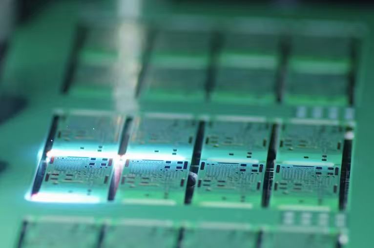
PCB Drilling Methods refer to the processes used to create vias, holes, and openings in the board that allow electrical connections between different layers or serve as mounting points for components. In multilayer PCB designs, these drilled holes can number in the thousands, each needing precise placement and controlled dimensions to maintain performance integrity.
The accuracy of drilling directly influences signal integrity, impedance control, and mechanical stability. For high-frequency PCBs, even a slight deviation in hole placement can result in reflection or attenuation of signals, leading to product malfunction.
Broadly speaking, PCB Drilling Methods must meet the following goals:
Accuracy – Achieving precise hole diameter and location.
Consistency – Ensuring repeatability across thousands of holes in mass production.
Efficiency – Balancing speed of production with quality output.
Cost-effectiveness – Optimizing capital investment in machinery versus operational expenses.
Over time, the industry has consolidated around three dominant PCB Drilling Methods, each with unique advantages and trade-offs:
Mechanical Drilling – The traditional workhorse of PCB fabrication.
Laser Drilling – A high-precision, non-contact method ideal for microvias.
Punching (Stamping) Drilling – A cost-effective option for high-volume, low-precision needs.
In the sections that follow, I will break down each of these three methods in detail, analyze their strengths, weaknesses, and industry use cases, and then compare them on the dual axis of cost versus precision.
The foundation of modern PCB manufacturing lies in drilling technology. While many experimental techniques have emerged over the decades, three PCB Drilling Methods have consistently dominated the industry: mechanical drilling, laser drilling, and punching (or stamping). Each method brings its own set of advantages, technical trade-offs, and best-fit applications.
In this section, I will explain the working principles of each method, highlight the situations where they excel, and critically analyze their contribution to both cost efficiency and precision control.
Mechanical drilling is the oldest and still the most widely used among PCB Drilling Methods. It relies on high-speed drilling machines equipped with micro drill bits, typically made from tungsten carbide, to physically cut holes through the board material.
Key Features of Mechanical Drilling
Capable of drilling through multiple layers simultaneously.
Handles a wide range of hole diameters, typically from 0.1 mm to several millimeters.
Highly reliable for through-hole vias and mounting holes.
Established ecosystem of equipment, tooling, and maintenance support.
Advantages
Mature and Proven Technology – Decades of use mean that mechanical drilling is a stable and well-understood process.
Wide Compatibility – Works across various PCB substrates, including FR4, polyimide, and high-frequency laminates.
Flexibility – Supports not only vias but also component lead holes and custom shapes.
Relatively Low Equipment Cost – Compared to laser systems, mechanical drilling machines are more affordable and widely available.
Limitations
Drill bits wear out, requiring frequent replacement.
Limited precision for microvias below 0.1 mm.
Slower throughput compared to punching for mass production.
Despite these limitations, mechanical drilling continues to dominate industries that require a balance between cost and performance, such as consumer electronics and automotive electronics.
Laser drilling represents the modern, high-precision alternative within PCB Drilling Methods. Instead of physically cutting the material, lasers vaporize the substrate to form clean, precise holes. CO₂ lasers and UV lasers are the two most common systems in industrial use.
Key Features of Laser Drilling
Ideal for microvias in high-density interconnect (HDI) boards.
Supports hole sizes as small as 20–30 microns.
Non-contact process reduces tool wear.
High repeatability and accuracy.
Advantages
Unmatched Precision – Perfect for microelectronics, 5G boards, and aerospace applications where sub-millimeter accuracy is critical.
No Mechanical Wear – Eliminates drill bit replacement, reducing downtime.
High Aspect Ratio Vias – Enables stacked vias and blind/buried vias in complex multilayer designs.
Scalability for Advanced Designs – As designs move toward miniaturization, laser drilling becomes indispensable.
Limitations
High initial capital investment in equipment.
Slower for larger-diameter holes.
Requires controlled environments to maintain accuracy.
Laser drilling has become the method of choice in sectors like telecommunications, aerospace, and medical devices, where failure due to poor drilling precision is unacceptable.
Punching, also known as stamping drilling, is the third major technique under PCB Drilling Methods. Instead of cutting with bits or vaporizing with lasers, this method uses a die-and-punch system to stamp out holes in one rapid motion.
Key Features of Punching
Extremely high throughput, suitable for mass production.
Best suited for single-layer or double-layer PCBs with simple layouts.
Limited to specific hole sizes defined by the die.
Advantages
Unparalleled Speed – Can process thousands of holes per second.
Lowest Cost Per Unit – Ideal for cost-sensitive, high-volume consumer products.
Simple Maintenance – Dies can be swapped quickly, minimizing downtime.
Scalable for Standardized Designs – Once tooling is prepared, production is extremely efficient.
Limitations
Not suitable for multilayer PCBs or advanced HDI boards.
Lacks the flexibility of mechanical or laser drilling.
Precision is limited by die quality.
Punching remains popular in industries such as toys, household electronics, and low-end consumer devices, where the priority is cost rather than precision.
Cost remains the single most influential factor when choosing among PCB Drilling Methods. While precision, reliability, and technological capability often determine feasibility, it is ultimately the cost structure that guides most manufacturing decisions. A balanced view requires analyzing both capital expenditure (CAPEX) and operational expenditure (OPEX) across the three major drilling approaches.
Mechanical Drilling
Equipment cost: Moderate.
Machines are widely available, with a mature supply chain.
Drill bits must be purchased and replaced regularly, adding to recurring costs.
Setup time is moderate, as operators need to align drill bits for accuracy.
Laser Drilling
Equipment cost: Very high.
A UV laser drilling machine can cost several times more than a mechanical drilling system.
Requires precise environmental control (temperature, vibration, dust).
Once installed, setup is relatively fast because no physical drill bits are needed.
Punching (Stamping) Drilling
Equipment cost: Low to moderate, depending on die complexity.
Dies must be custom-manufactured for each PCB design.
Initial tooling cost is significant, but once produced, setup is fast and cheap.
Summary:
Mechanical drilling has the best balance of upfront cost and versatility.
Laser drilling demands the highest capital investment, but pays off for high-value, high-precision boards.
Punching has low ongoing cost, but only when design volumes are massive.
Mechanical Drilling
Drill bits wear quickly, sometimes after only a few hundred holes.
Labor cost is higher due to operator monitoring and machine adjustments.
Energy consumption is moderate.
Laser Drilling
No consumable drill bits, but lasers require periodic calibration and servicing.
High electricity usage, especially for CO₂ lasers.
Lower operator intervention, but maintenance requires skilled technicians.
Punching Drilling
Operational costs are extremely low once dies are fabricated.
Tool wear is minimal, but die replacement can be costly if design changes frequently.
Labor requirements are minimal since the process is mostly automated.
Summary:
Mechanical drilling incurs steady operational costs.
Laser drilling has higher energy and maintenance costs, offset by fewer consumables.
Punching is cheapest per unit, but inflexible when production volumes are low or designs change often.
Mechanical Drilling: Scales moderately well. Costs rise with hole density because of drill bit wear and machine time. Best suited for medium-to-large production volumes.
Laser Drilling: Scales effectively for high-tech, low-to-medium volumes where precision outweighs unit cost. For example, medical devices and aerospace boards often accept higher per-unit cost.
Punching Drilling: Scales perfectly for mass production. Once tooling is prepared, unit costs drop dramatically. This is why low-cost consumer electronics often rely on this approach.
| Method | Equipment Cost | Operational Cost | Scalability | Best-fit Volume |
|---|---|---|---|---|
| Mechanical | Moderate | Moderate | Medium | Medium–Large |
| Laser | Very High | High | High (low-medium volume) | Low–Medium |
| Punching | Low–Moderate | Very Low | Very High | Very Large |
From my perspective, the cost debate is not as straightforward as it appears. Many decision-makers in the PCB industry fall into the trap of choosing the cheapest method upfront, only to face long-term losses due to product failures, redesigns, or yield issues.
For example:
A startup manufacturing IoT sensors might be tempted by mechanical drilling for its affordability, but if their design requires microvias, the rework costs could easily surpass the savings.
On the other hand, a large consumer electronics company making remote controls may find punching irresistible, as its per-unit cost is negligible once dies are set.
This is why selecting the right PCB Drilling Methods requires aligning cost models with product lifecycle goals. It’s not just about initial savings, but about value over time.
Precision is the invisible thread that determines whether a PCB will function flawlessly or fail under operational stress. Among all PCB Drilling Methods, the level of achievable accuracy and consistency varies dramatically. Understanding these differences is crucial when balancing cost with long-term performance.
Mechanical drilling has long been the backbone of the PCB industry, but its precision is inherently limited by the physical nature of drill bits.
Precision Characteristics:
Typical hole tolerance: ±25–50 microns.
Hole diameter range: 0.1 mm to several millimeters.
Drill bit wander can cause slight misalignment.
Aspect ratio (hole depth to diameter) is limited, usually up to 10:1.
Defect Risks:
Burr formation around the hole edges.
Bit breakage leading to incomplete or oversized holes.
Misregistration in multilayer stacks due to tool wear.
Reflection:
Mechanical drilling achieves acceptable precision for most mainstream PCBs, but for advanced HDI boards requiring microvias, its limitations quickly become apparent.
Laser drilling is the undisputed leader in precision among PCB Drilling Methods, especially in the domain of high-density interconnect (HDI).
Precision Characteristics:
Typical hole tolerance: ±10 microns or better.
Hole diameter as small as 20–30 microns (microvias).
Perfect for blind and buried vias.
Clean hole walls with minimal burrs.
Defect Risks:
Thermal damage if energy settings are miscalibrated.
Over-etching or tapering in thicker materials.
Sensitive to dust and vibration in the environment.
Reflection:
For applications where signal integrity, high frequency, or miniaturization is critical, laser drilling is unmatched. However, the extremely high precision comes with significant cost implications, which we analyzed in the previous section.
Punching, though incredibly cost-effective, lags behind in precision compared to mechanical and laser drilling.
Precision Characteristics:
Typical hole tolerance: ±75–100 microns.
Limited to predefined hole diameters set by the die.
Edge quality depends heavily on die sharpness.
Defect Risks:
Deformation of hole edges if the die is worn.
Misalignment when handling multilayer boards.
Inconsistent hole roundness at high volumes.
Reflection:
Punching is highly effective for large, simple boards where hole tolerances are not mission-critical. But for high-frequency or miniaturized PCBs, this method cannot meet the necessary precision requirements.
| Method | Hole Tolerance | Minimum Hole Size | Typical Defects | Best Precision Application |
|---|---|---|---|---|
| Mechanical | ±25–50 µm | ~0.1 mm | Burrs, misregistration | General multilayer boards |
| Laser | ±10 µm | ~20–30 µm | Thermal damage, tapering | HDI, aerospace, telecom |
| Punching | ±75–100 µm | ~0.2 mm (fixed) | Edge deformation, wear | Low-cost consumer boards |
Precision, in my experience, is often misunderstood by decision-makers. Many equate higher precision with always being better. While true in theory, in practice, “good enough precision” is often the optimal choice.
For example:
A remote control PCB does not need ±10 µm precision. Here, punching provides the best cost-performance balance.
A 5G communication module, however, cannot tolerate even ±25 µm deviation because microvia misalignment could destroy signal performance.
For automotive safety systems, where reliability is non-negotiable, manufacturers often choose mechanical drilling with rigorous quality checks, avoiding unnecessary expenses of laser drilling unless the design requires it.
The practical relevance of PCB Drilling Methods becomes clear when examining their adoption across industries. Different sectors demand varying balances of cost, precision, reliability, and scalability. No single drilling method dominates universally; instead, the choice is always application-driven.
Consumer electronics, such as smartphones, laptops, gaming consoles, and home appliances, form one of the largest markets for PCB manufacturing.
Mechanical Drilling: Still widely used for multilayer boards in laptops, televisions, and mid-range smartphones. Offers sufficient precision without excessive cost.
Laser Drilling: Dominant in high-end smartphones and wearables, where miniaturization and HDI microvias are required.
Punching Drilling: Preferred for low-cost devices like remote controls, calculators, and toys, where precision requirements are minimal but unit cost is critical.
Why This Choice?
Consumer electronics demand both scale and cost efficiency. High-volume products tend to use punching or mechanical drilling, while premium products requiring HDI boards adopt laser drilling.
Modern vehicles rely heavily on electronics for everything from safety systems to infotainment. Reliability is critical, as PCB failures can directly impact safety.
Mechanical Drilling: Extensively used in automotive ECUs (engine control units), safety sensors, and dashboard electronics. Offers robust balance of cost and reliability.
Laser Drilling: Gaining adoption in advanced driver-assistance systems (ADAS) and radar modules where high-frequency signals demand microvias.
Punching Drilling: Rarely used in automotive, as safety standards do not allow high tolerance variation.
Why This Choice?
The automotive industry prefers mechanical drilling due to its maturity, reliability, and suitability for medium-precision needs. For next-generation ADAS and EV power electronics, laser drilling is becoming more relevant.
The telecom sector, particularly with the rise of 5G and high-frequency RF applications, requires boards with extreme precision.
Laser Drilling: The undisputed leader, as microvias are essential for HDI designs that support GHz frequencies.
Mechanical Drilling: Sometimes used for larger connectors or mixed-technology boards.
Punching Drilling: Not viable due to poor precision.
Why This Choice?
In telecom, signal integrity outweighs cost, making laser drilling the primary method of choice.
Medical devices such as pacemakers, diagnostic equipment, and wearable health monitors require miniaturization and reliability.
Laser Drilling: Widely adopted for implantable devices and advanced diagnostic electronics due to microvia capability.
Mechanical Drilling: Used for less compact designs such as large diagnostic machines.
Punching Drilling: Unsuitable, as precision is critical to patient safety.
Why This Choice?
For life-critical applications, the cost is secondary to precision and reliability. Hence, laser drilling dominates medical electronics.
Aerospace and defense systems operate under extreme conditions, demanding uncompromising reliability.
Laser Drilling: Used in radar, avionics, and satellite systems requiring ultra-precise microvias.
Mechanical Drilling: Still common in power management and rugged systems where larger holes are sufficient.
Punching Drilling: Entirely unsuitable due to lack of reliability.
Why This Choice?
Aerospace manufacturers prefer laser drilling for cutting-edge systems but still rely on mechanical drilling where cost savings are possible without compromising safety.
| Industry | Mechanical Drilling | Laser Drilling | Punching Drilling |
|---|---|---|---|
| Consumer Electronics | High (mid-range products) | High (premium devices) | High (low-cost goods) |
| Automotive | Very High | Growing | Low |
| Telecommunications | Low | Very High | None |
| Medical Devices | Medium | Very High | None |
| Aerospace/Defense | High | Very High | None |
Having observed trends across industries, I find that the choice of drilling method often mirrors the product’s mission:
If the mission is mass adoption → Punching wins.
If the mission is balanced performance and cost → Mechanical drilling wins.
If the mission is maximum reliability and miniaturization → Laser drilling wins.
It is also clear that laser drilling is steadily expanding as products continue to shrink and demand higher frequencies. Still, mechanical drilling retains dominance due to its versatility and lower cost, while punching will always remain a niche for ultra-low-cost, high-volume applications.
Selecting the right PCB Drilling Methods is a strategic decision that shapes both the quality and profitability of electronic products. As we explored throughout this article, the choice between mechanical drilling, laser drilling, and punching is never arbitrary—it is dictated by the specific technical requirements, production volume, cost considerations, and end-use applications.
Understanding PCB Drilling Methods
Mechanical drilling remains versatile and cost-effective for medium-precision applications.
Laser drilling excels in microvia precision, high-density interconnects, and high-frequency circuits.
Punching is ideal for low-cost, high-volume consumer boards with minimal precision requirements.
Precision vs Cost Trade-offs
Maximum precision often comes with higher costs, both in capital investment and operation.
Mechanical drilling provides a balanced compromise, while punching optimizes cost but sacrifices precision.
Laser drilling is justified where precision and reliability cannot be compromised, such as aerospace, medical, and telecom applications.
Industry Applications Guide Decision-Making
Consumer electronics: Punching and mechanical drilling for low-cost or mid-range devices, laser for premium products.
Automotive: Mechanical drilling dominates, with laser for advanced systems.
Telecom, Medical, Aerospace: Laser drilling is essential for microvias and signal integrity.
The Power of Hybrid Approaches
Many modern PCBs combine drilling methods within the same board or stack to optimize cost, precision, and throughput.
Hybrid strategies allow manufacturers to adapt to varying layer requirements efficiently.
Partnering with Experienced Suppliers
Suppliers like JM PCB provide expertise and multi-method capabilities, enabling companies to select the optimal drilling method for each layer or component.
This reduces risk, improves yield, and accelerates production.
Answer:
Rolled copper foil is produced by mechanically rolling copper into thin sheets, offering better surface quality and mechanical strength.
Electrolytic copper foil is deposited via an electrolytic process and is more flexible and cost-effective.
Answer:
No. Laser drilling is excellent for microvias and high-density boards, but mechanical drilling remains more cost-effective for medium to large holes and high-volume production.
Answer:
Punching relies on physical dies, which can deform board edges and produce slightly irregular holes, especially in multilayer boards.
Die wear over time increases the probability of misalignment or burrs.
Answer:
High-frequency boards (RF, 5G, aerospace) require tight tolerances, smooth hole walls, and precise microvias.
Laser drilling is usually the only method that meets these requirements, while mechanical or punching methods may introduce signal degradation.
Answer:
Yes. Suppliers with capabilities in mechanical, laser, and punching drilling allow companies to test, prototype, and produce hybrid boards efficiently.
This flexibility can reduce lead times, optimize cost, and improve yield.


Connect to a Jerico Multilayer PCB engineer to support your project!
Request A Quote


 Quote
Quote